


Intro to Boron Nitride Ceramics: A Special Course of High-Tech Materials
Boron nitride ceramic items have actually become an essential class of sophisticated porcelains, identified by their distinct mix of thermal conductivity, electric insulation, chemical inertness, and mechanical security at severe temperatures. Unlike conventional oxide or carbide-based porcelains, boron nitride (BN) exists in several crystalline kinds– most notably hexagonal (h-BN), cubic (c-BN), and wurtzite (w-BN)– each offering unique homes fit for specialized applications. From high-temperature crucibles to semiconductor parts and quantum tools, BN porcelains are redefining performance limits across markets ranging from aerospace to microelectronics.
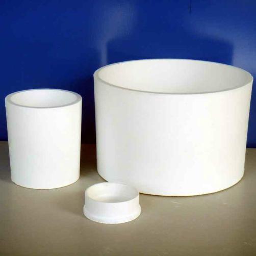
(Boron Nitride Ceramic)
Structural Properties and Polymorphic Variations of Boron Nitride Ceramics
The versatility of boron nitride stems from its capacity to embrace different crystal structures, each with customized physical and chemical features. Hexagonal boron nitride (h-BN), usually described as “white graphite,” includes a layered framework that imparts superb lubricity, low rubbing, and high thermal conductivity while keeping electrical insulation. Cubic boron nitride (c-BN), second just to ruby in solidity, is commonly utilized in reducing tools and rough applications. Wurtzite BN (w-BN) displays piezoelectric buildings, making it ideal for high-pressure sensors and optoelectronic devices. These polymorphs enable the style of extremely specialized ceramic products adapted to requiring industrial settings.
Manufacturing Techniques and Product Challenges
Making high-grade boron nitride ceramic items includes exact powder synthesis, shaping, and sintering techniques. h-BN is commonly fabricated through warm pushing or spark plasma sintering, while c-BN needs high-pressure, high-temperature (HPHT) approaches to support its cubic stage. Attaining thick, defect-free BN ceramics continues to be an obstacle because of the product’s naturally low self-diffusivity and propensity toward porosity. Ingredients such as yttria or alumina are frequently introduced to boost densification without jeopardizing thermal or electric efficiency. Recurring research focuses on additive manufacturing, nanostructuring, and crossbreed compounds to expand the series of practical geometries and functionalities.
Applications in Electronic Devices, Semiconductors, and Thermal Administration Solution
Among the most considerable functions of boron nitride ceramic items depends on the electronic devices and semiconductor industries, where thermal management and electric isolation are critical. h-BN substratums are significantly used in power components, RF components, and LED plans as a result of their premium thermal conductivity and dielectric homes. In semiconductor crystal growth procedures– such as Czochralski drawing or directional solidification– BN crucibles make sure contamination-free melt handling. In addition, thin-film BN layers serve as diffusion barriers and passivation layers in integrated circuits, boosting tool dependability under extreme operating problems.
Use in Aerospace, Protection, and Nuclear Technologies
Boron nitride ceramic items also play a crucial function in aerospace, protection, and atomic energy systems. Their neutron-absorbing abilities make them excellent for control poles and protecting materials in atomic power plants. In hypersonic trip and area expedition, BN compounds give light-weight, thermally steady elements efficient in standing up to re-entry temperature levels surpassing 2000 ° C. Armed force applications consist of radar-transparent radomes, projectile nose cones, and armor-piercing penetrators made from c-BN-reinforced porcelains. As national protection and room industries develop, require for BN-based materials is anticipated to grow dramatically.
Developments in Mechanical and Commercial Handling Tools
( Boron Nitride Ceramic)
Cubic boron nitride (c-BN) has changed machining and metalworking industries because of its exceptional firmness and thermal security. c-BN cutting devices surpass conventional tungsten carbide and also some ruby tools when machining ferrous alloys, as they do not chemically react with iron at heats. This makes them crucial in automobile and aerospace manufacturing, where precision and tool durability are vital. Innovations in layer technologies and composite tool styles continue to press the limitations of c-BN’s performance, allowing much faster machining speeds and extended tool life in high-volume production setups.
Environmental and Economic Considerations
In spite of their high-performance advantages, boron nitride ceramic products deal with financial and environmental difficulties. Manufacturing costs continue to be raised due to complex synthesis routes and minimal economic situations of range compared to even more well established technological ceramics like silicon nitride or light weight aluminum oxide. Recycling and end-of-life disposal methods are still in very early growth, though interest in circular manufacturing models is expanding. Researchers are exploring alternate basic material resources, bio-derived binders, and multiple-use mold and mildew technologies to decrease the environmental footprint of BN ceramic manufacturing while improving cost competitiveness.
Market Trends and Worldwide Sector Development
The international market for boron nitride ceramic items is experiencing stable growth, driven by raising demand from the semiconductor, defense, and tidy power sectors. Asia-Pacific leads in usage, especially in China and Japan, where financial investments in next-generation electronics and photovoltaics are increasing. North America and Europe comply with very closely, supported by government-backed R&D programs in quantum computing, blend energy, and hypersonic lorry development. Principal are broadening production capacity, forming strategic collaborations, and investing in digital procedure optimization to satisfy climbing global demand for high-performance BN ceramic options.
Future Leads: Integration with Smart Manufacturing and Advanced Products Science
Looking in advance, boron nitride ceramic products are positioned to play a central duty in the evolution of clever manufacturing, AI-driven materials design, and next-generation electronic systems. Advancements in additive manufacturing are allowing the construction of facility BN geometries formerly unattainable via conventional approaches. Assimilation with IoT-enabled sensors and anticipating upkeep platforms will boost real-time monitoring of BN elements in high-stress settings. In addition, arising research right into 2D BN nanosheets, heterostructures, and quantum-confined systems promises advancements in optoelectronics, spintronics, and ultra-fast computing, additional sealing BN porcelains as foundational products for future technical technology.
Supplier
Advanced Ceramics founded on October 17, 2012, is a high-tech enterprise committed to the research and development, production, processing, sales and technical services of ceramic relative materials and products. Our products includes but not limited to Boron Carbide Ceramic Products, Boron Nitride Ceramic Products, Silicon Carbide Ceramic Products, Silicon Nitride Ceramic Products, Zirconium Dioxide Ceramic Products, etc. If you are interested, please feel free to contact us.(nanotrun@yahoo.com)
Tags: boron nitride ceramic, ceramic boron nitride, machining boron nitride
All articles and pictures are from the Internet. If there are any copyright issues, please contact us in time to delete.
Inquiry us

